|
PST Series - Thermal Test Die with Resistive Heaters |
Nbr
Pads |
Features |
Pitch |
Die Size
(mm) |
Die
Thickness |
Waffle Tray
Qty |
5" Wafer
(125mm)
Die Qty |
Bondable
Pad |
Single Die
Part Number |
Unsawn Wafer
Part Number |
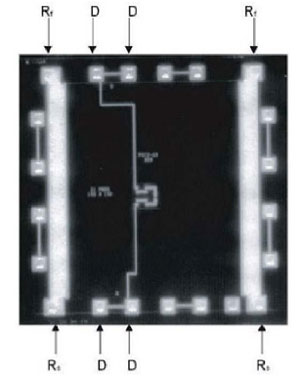
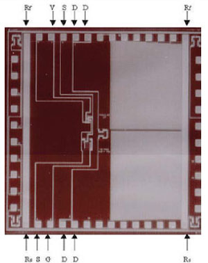
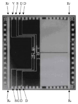
Photo |
Schematic |
| 32 |
Heating Elements
2x Resistive Heaters
Temperature Sense
Kelvin-Diode-Resistor
5x Serial Diode Sensor |
X=230µm
Y=230µm |
2.5mm
100 mil |
100~635µm
4~25 mil |
100 Die
2" Tray |
1600 Die
5" Wafer |
ø102µm
4.0 mil |
PST1-G2.5A |
PSTW1-G2.5A |
 |
 |
□122µm
4.8 mil |
PST1-B2.5A |
PSTW1-B2.5A |
| 21 |
Heating Elements
2x Resistive Heaters
Temperature Sense
5x Serial Diode Sensor |
X=460µm
Y=690µm |
3.81mm
150 mil |
100~635µm
4~25 mil |
64 Die
2" Tray |
700 Die
5" Wafer |
ø100µm
4.0 mil |
PST2-G3.8A |
PSTW2-G3.8A |
 |
 |
Ø127µm
5.5 mil |
PST2-N3.8A |
PSTW2-N3.8A |
□150µm
5.9 mil |
PST2-C3.8A |
PSTW2-C3.8A |
| 76 |
Heating Elements
2x Resistive Heaters
Temperature Sense
Kelvin-Diode-Resistor
5x Serial Diode Sensor |
X=231µm
Y=231µm |
5.08mm
200 mil |
100~635µm
4~25 mil |
36 Die
2" Tray |
340 Die
5" Wafer |
□120µm
4.7 mil |
PST3-B5A |
PSTW3-B5A |
 |
 |
| 48 |
Heating Elements
2x Resistive Heaters
Temperature Sense
Kelvin-Diode-Resistor
5x Serial Diode Sensor
Center & each corner |
X=381µm
Y=508µm |
6.35mm
250 mil |
100~635µm
4~25 mil |
25 Die
2" Tray |
236 Die
5" Wafer |
Ø100µm
4.0 mil |
PST4-G6.3A |
PSTW4-G6.3A |
 |
 |
| 60 |
Heating Elements
2x Resistive Heaters
Temperature Sense
Kelvin-Diode-Resistor
5x Serial Diode Sensor
Center & each corner |
X=381µm
Y=508µm |
7.8mm
306 mil |
100~635µm
4~25 mil |
64 Die
4" Tray |
146 Die
5" Wafer |
Ø182µm
7.2 mil |
PST5-U7.8A |
PSTW5-U7.8A |
 |
 |
| 82 |
Heating Elements
2x Resistive Heaters
Temperature Sense
Kelvin-Diode-Resistor
5x Serial Diode Sensor
Center & each corner |
X=381µm
Y=508µm |
10mm
400 mil |
100~635µm
4~25 mil |
49 Die
4" Tray |
80 Die
5" Wafer |
□183µm
7.2 mil |
PST6-D10A |
PSTW6-D10A |
 |
 |
 |
| Note 1: Standard Die thickness 635um (25MIL) |
Note 2: Thinning available: 500um (20MIL), 430um (17MIL), 360um (14MIL), 250um (10MIL), 200um (8MIL), 150um (6MIL), 100um (4MIL) |
Note 3: JEDEC Moisture Sensitivity Level MSL-1. |
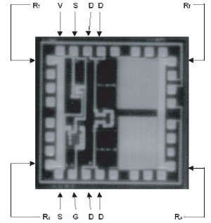
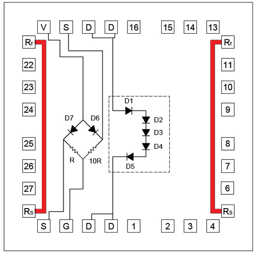
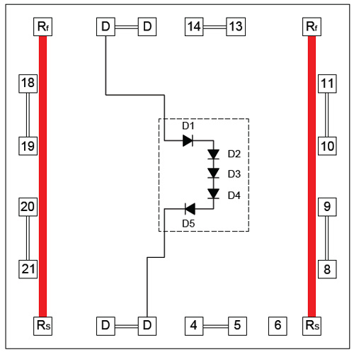
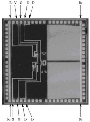
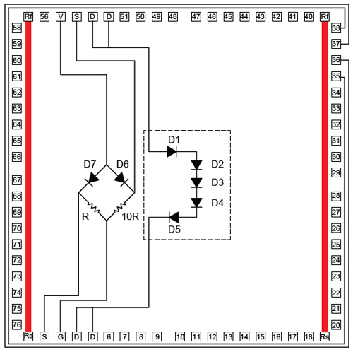
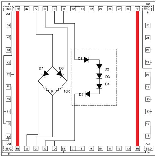
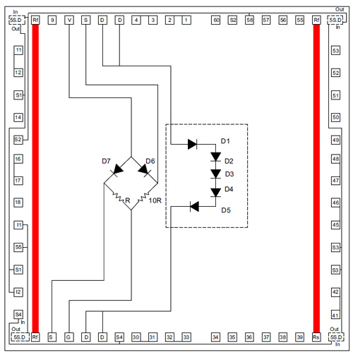
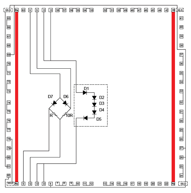
Note 4: Applications: Use PST series test die to heat semicoductor packages and measure changes in temperatures, ΘJC and ΘJA. A four pad layout (V-S-S-G) allows Kelvin connections. A temperature monitoring circuit uses a bridge network. Chips include serial five-diode temperature sense network. Power up to 2.5W per die. |
Note 5: Stack Die: Multiple die can be thinned to 127um (5mils) and stacked in offset pryamid fashion for easy wire bonding. Use 0.038mm (1.5mil) thick non-conductive die attach material between PST-2 to PST-4 and PST-4 to PST-6. Use electrically conductive die attach material between PST-6 and the substrate. |
Note 6: Resistive Heaters: All die have dual resistive heaters connection Rs to Rf. Typically powered 0 to 3.5V at 160mA (0.5W).
Multiple die can be run in parallel to increase heat source. Customers may determine maximum power rating by experimentation. 500mA current limiting power source is recommended for safety. Maximum power rating is not stated. |
Note 7: Voltage Sense: 5.0~15V input (with a controlled current supply) may be applied across the bridge diodes and resistors at pads V to G and/or across D to D. Voltage sensing (output) is measured from pads V to S and pads S to G. Daisy chain pads are optionally used only for monintoring continuity with an ohm meter (near zero ohms). |
Note 8: Temperature Sense Network: All PST series die have serial five-diodes to sense temperature. |
Note 9: Temperature Change: Temperature can be monitored by measuring the forward voltage across the diodes. Forward voltage will drop approximately 2mV for each degree °C rise above ambient temperature (25°C). Probe between pad "V" and pad "S" on the die. See map of pads to located V and S on the dies. |
Note 10: Meets JEDEC specification EIA/JESD51-4. |
| |
| |
|