| NASA GSFC-STD-6001: |
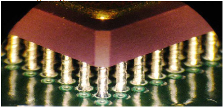
| IBM Solder Column: Pb90Sn10 2.21mm L x 0.51mm diameter and 1.62mm L x 0.89mm diameter. |
| Copper Wrapped Solder Column: Pb80Sn20, Sn-plated Cu Wrap, Sn63Pb37 Finish. 2.21mm L x 0.51mm diameter |
| |
| Component Inspection: |
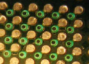
| Colpanarity: Less than +/-0.15mm (0.0059-inch) |
| Single Column Tilt: An individual column shall not be bent more than 5° relative to other columns |
| Multiple Column Tilt: Tilt is acceptable if all columns are tilted uniformally up to maximum 10° |
| Visual Inspection: Use 10X magnification |
| |
| PWB Board Requirements: |
| PWB Board Material: Polyimide recommended due to lower CTE compared with epoxy-class boards. |
| PWB Allowed Finish: Tin-lead solder or Electroless-Nickel, Immersion Gold (ENIG). Maximum 0.254µm (10 micro-inch) gold. |
| PWB Prohibited Finish: Pure tin or other lead free surface plating is not allowed. |
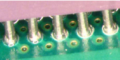
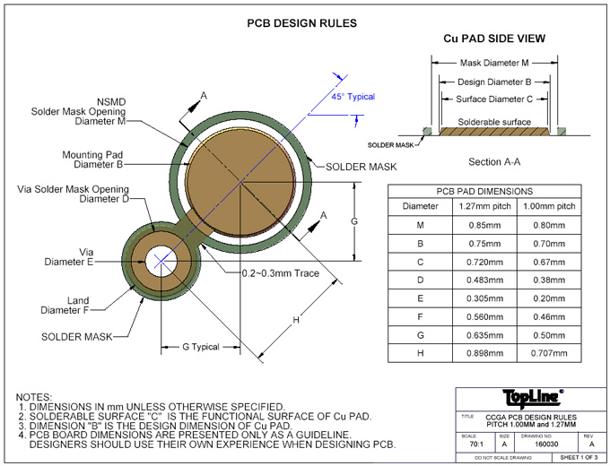
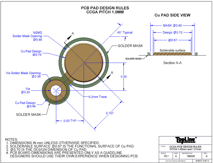
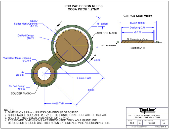
| PWB Pad Diameter: Non-Solder Masked Defined pads (NSMD) minimum 120% of solder column diameter |
| PWB Component Courtyard: 0.3-inch (7.62mm) minimum clearance to allow sufficient clearance for rework. |
| |
| Assembly Requirements: |
| Underfill: Not allowed under the CCGA component. |
| Solder Paste Stencil: Laser cut stencils are recommend, instead of chem-etched stencils. |
| |
| Rework Requirements: |
| Prohibited Reuse of Columns: Columns shall not be reused even if they remain attached to the CCGA part after removal from the board. |
| |
| Process Validation Testing: |
| Electrical Continuity: Use daisy chained connections at -55°C , +100°C and +25°C to identify a failed attachment. |
| |
| ECCN: EAR99 Export Administration Regulations (EAR) |
| HS Code: 8542.90.0000 ELECTRONIC INTEGRATED CIRCUITS AND MICROASSEMBLY PARTS |
| HS Code: 8311.30.3000 Lead-Tin Solders |
| ITAR: Solder columns and dummy daisy chain CCGA are not
restricted. |
| |
| |